Processes and Materials
Overview of our Capabilities
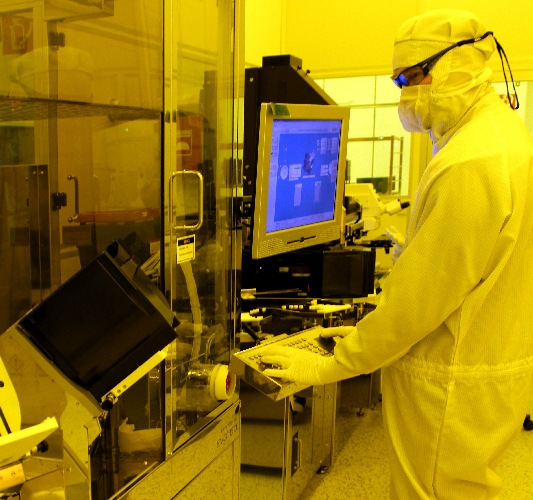
Lithoglas operates wafer fab cleanrooms offering a broad range of equipment and material capabilities.
- Cleanroom Class 10 and 1000
- Wafer Sizes: 200mm, 150mm, 100mm (not supported in all processes)
- Wafer Cleaning (wet, dry)
- Wet Etching of Silicon and Glass
- Laser Structuring of Borosilicate and Silica Glasses
- CD Microscopes, Automatic Optical Inspection, Thickness Measurement, Profilometer
- PVD Deposition of SiO2 and Al2O3
- Lithography – Spin-On and Spray Resist Coating (positive and negative tone)
- Lithography – Mask Alignment (front and backside, 2 mic resolution)
- Wafer Bonding (Anodic and Fusion)
- Metal Deposition of Al, Cr, CrNi, Au, WTi
- Thermal Oxide Deposition
- LPCVD and PECVD Silicon Nitride deposition
- Wafer Dicing

